STM32C0
Table of contents
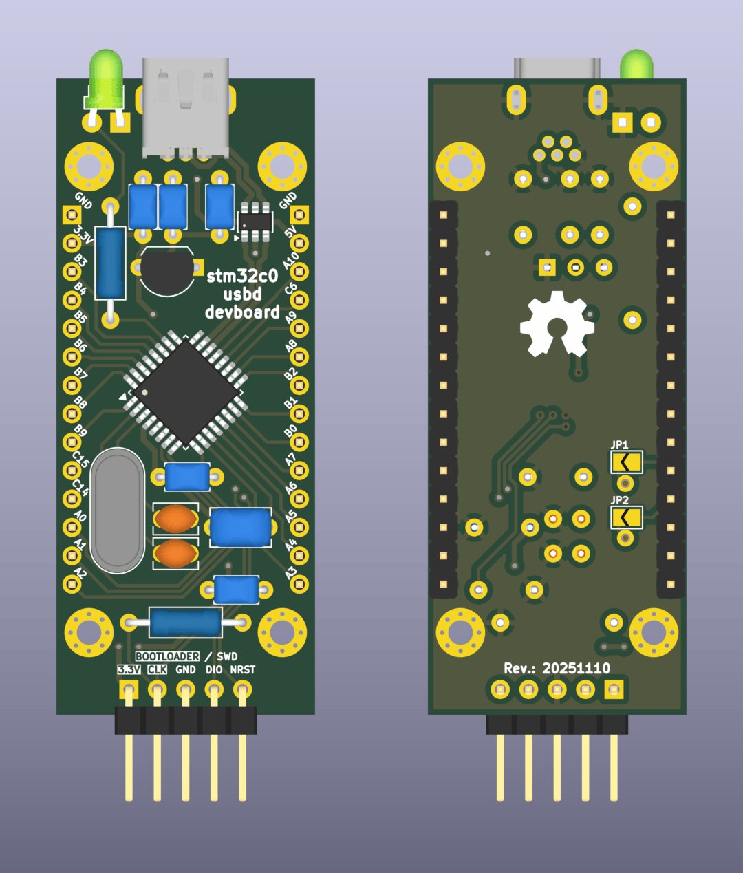
The STM32C0 variant is based on the STM32C071K8T6 (ARM Cortex-M0+, 48 MHz) -- the newest addition to the lineup. Like the STM32F0 variant, it runs crystal-free using the HSIUSB48 internal oscillator self-calibrated via USB SOF packets, with an optional HSE crystal footprint on the board. The Cortex-M0+ core offers improved power efficiency over the Cortex-M0 in the F0, and this variant provides the largest pin count of the three boards with 2x14 headers exposing 28 GPIO + power pins.
Current revision (20251110)
STM32C0 USB Development Board
Resources:
KiCad source files are available in the repository under pcb/stm32c0-usbd-devboard/. A KiCad symbol for this board (stm32c0-usbd-devboard) is provided in symbols/stm32-usbd-devboards.kicad_sym.
Supported microcontrollers
The board uses the CMSIS device identifier STM32C071xx.
| Part number | Flash | RAM |
|---|---|---|
| STM32C071K8T6 | 64 KB | 24 KB |
Pinout
Two 1x14 pin headers at 2.54 mm pitch -- the largest of the three variants.
| J3 (Left) | Pin | J4 (Right) |
|---|---|---|
| GND | 1 | GND |
| 3V3 | 2 | +5V |
| B3 | 3 | A10 |
| B4 | 4 | C6 |
| B5 | 5 | A9 |
| B6 | 6 | A8 |
| B7 | 7 | B2 |
| B8 | 8 | B1 |
| B9 | 9 | B0 |
| C15 | 10 | A7 |
| C14 | 11 | A6 |
| A0 | 12 | A5 |
| A1 | 13 | A4 |
| A2 | 14 | A3 |
Note
Pins C14 and C15 are unconnected by default. Closing solder bridge JP1 connects board pin C15 to GPIO PC15. Closing JP2 connects board pin C14 to GPIO PC14. These solder bridges must not be closed if an HSE crystal is installed, as PC14/PC15 are shared with the crystal oscillator pins.
Clocking
The default clock source is the HSIUSB48 internal oscillator at 48 MHz, self-calibrated via USB SOF packets from the host -- the same approach used by the F0 variant. No external crystal is needed for USB operation. For USB, firmware must enable the Clock Recovery System (CRS) peripheral synced from USB so that SOF packets continuously calibrate HSIUSB48. Without CRS enabled, the oscillator frequency will drift outside USB tolerance and communication will fail. CRS synced from USB is usually already enabled on reset.
An optional 48 MHz HSE crystal (Y1, HC49 package) can be installed if HSE is required for your application. When using HSE, it serves as the system clock directly -- STM32C0 devices have no PLL -- and HSIUSB48 is not needed. The solder bridges JP1/JP2 must remain open when HSE is installed, since PC14/PC15 serve as the oscillator pins.
The maximum system clock frequency is 48 MHz.
SWD and DFU bootloader
The C0 variant uses a combined SWD + Bootloader header (J2) -- a single 5-pin vertical header that consolidates the separate SWD and bootloader headers found on the F0 and G4 variants.
| Pin | Signal |
|---|---|
| 1 | 3V3 |
| 2 | SWCLK |
| 3 | GND |
| 4 | SWDIO |
| 5 | NRST |
Note
On STM32C0 devices, the BOOT0 pin behavior needs to be configured via option bytes according to the STM32: Enable Legacy Boot document. Refer to the STM32C0 reference manual and the generic Hardware Build Manual for details on USB DFU flashing.
Board-specific build notes
- HSE crystal (Y1): Optional. 48 MHz, HC49 package. Only install if HSE is required.
- Solder bridges JP1/JP2: Open by default. Close only if the HSE crystal is not installed, to route PC14/PC15 to the header pins.
- LED (D1): Green 3 mm PTH, horizontal mount.
For the complete build process, see the generic Hardware Build Manual.
Firmware development
For project setup, build system configuration, toolchain usage, and flashing instructions, refer to the cmake-cmsis-stm32 documentation. The CMSIS device identifier for this board is STM32C071xx.
For register-level details on clock configuration, CRS, USB peripheral, and GPIO, refer to the STM32C0 reference manual (RM0490).