STM32F0
Table of contents
The STM32F0 variant is based on the STM32F042K4T6/K6T6 (ARM Cortex-M0, 48 MHz) in LQFP-32 package -- the simplest board in the lineup for straightforward USB projects. The STM32F042 integrates an HSI48 internal oscillator that is automatically calibrated by the USB host through SOF packets, enabling crystal-free USB device operation. When no HSE crystal is installed, the two crystal pins (PF0, PF1) can be repurposed as GPIO by closing solder bridges JP1 and JP2.
Current revision (20250412)
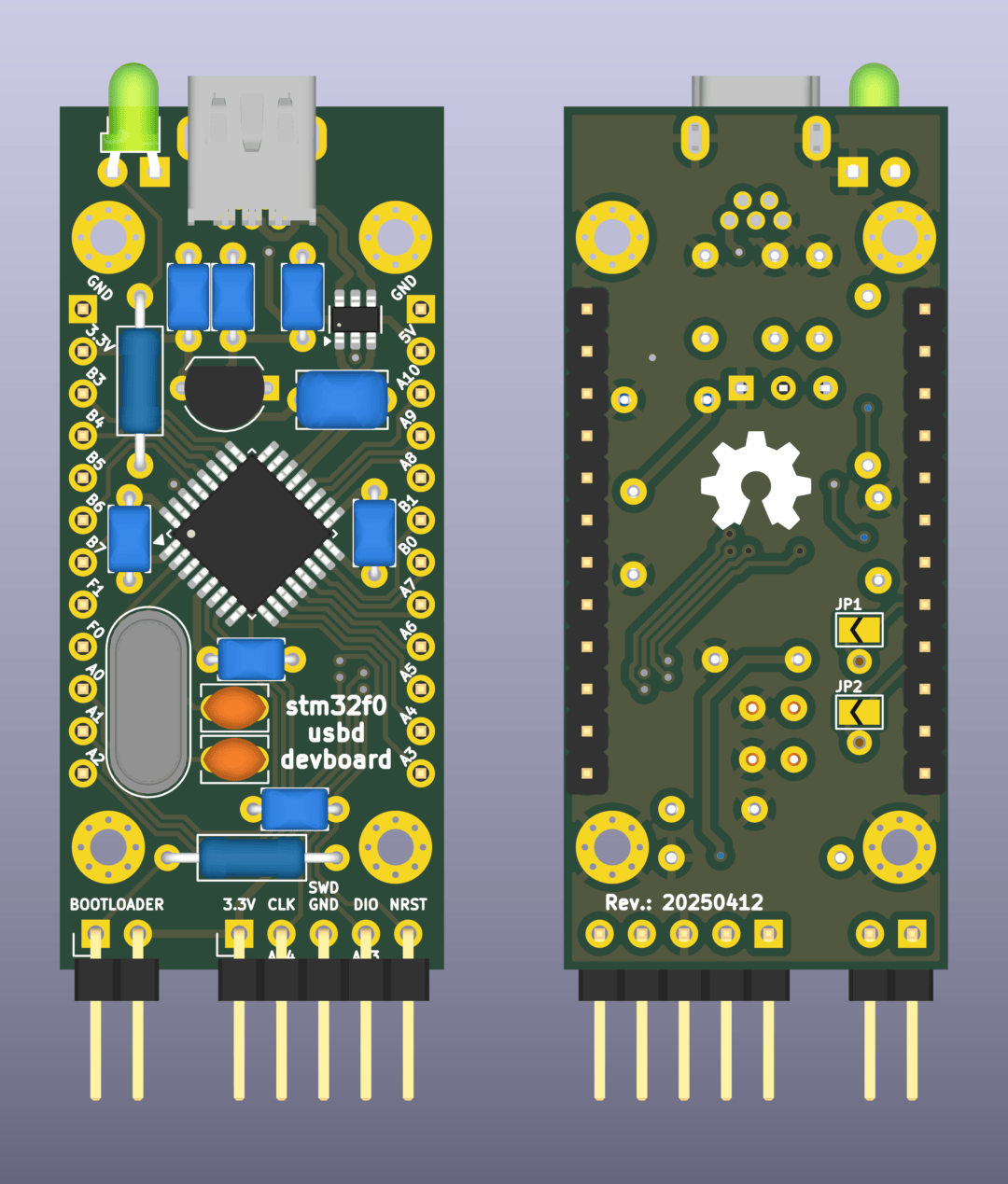
STM32F0 USB Development Board
Resources:
KiCad source files are available in the repository under pcb/stm32f0-usbd-devboard/. A KiCad symbol for this board (stm32f0-usbd-devboard) is provided in symbols/stm32-usbd-devboards.kicad_sym.
Supported microcontrollers
Both parts share the CMSIS device identifier STM32F042x6 and differ only in flash size.
| Part number | Flash | RAM |
|---|---|---|
| STM32F042K4T6 | 16 KB | 6 KB |
| STM32F042K6T6 | 32 KB | 6 KB |
Warning
The CMSIS device identifier selects headers and startup code, but the linker script determines the memory layout. STM32F042x6 covers both the K4 (16 KB) and K6 (32 KB) parts. You must use a linker script that matches the actual chip populated on your board -- using a linker script for the larger flash variant will compile and link without errors but may produce firmware that writes beyond the physical flash.
Pinout
Two 1x12 pin headers (2.54 mm pitch) provide power and 20 GPIO.
| J3 (Left) | Pin | J4 (Right) |
|---|---|---|
| GND | 1 | GND |
| 3V3 | 2 | +5V |
| B3 | 3 | A10 |
| B4 | 4 | A9 |
| B5 | 5 | A8 |
| B6 | 6 | B1 |
| B7 | 7 | B0 |
| F1 | 8 | A7 |
| F0 | 9 | A6 |
| A0 | 10 | A5 |
| A1 | 11 | A4 |
| A2 | 12 | A3 |
Note
Pins F0 and F1 are unconnected by default. Closing solder bridge JP1 connects board pin F1 to GPIO PF1. Closing JP2 connects board pin F0 to GPIO PF0. These solder bridges must not be closed if an HSE crystal is installed, as PF0/PF1 are shared with the crystal oscillator pins.
Clocking
The STM32F042 supports two clock sources for USB operation at 48 MHz:
- HSI48 (default) -- 48 MHz internal RC oscillator, self-calibrated via USB SOF packets from the host. This is the recommended configuration for most USB device applications. Firmware must enable the Clock Recovery System (CRS) peripheral synced from USB so that incoming SOF packets continuously trim HSI48. Without CRS, the oscillator frequency drifts outside USB tolerance and communication will fail. CRS synced from USB is usually already enabled on reset.
- HSE crystal (optional) -- 8 MHz external crystal (HC49 package), multiplied to 48 MHz via the PLL. Useful when the board is USB-powered but not actively communicating over USB, making SOF-based calibration unavailable. When HSE is used as the system clock source, HSI48 is not needed.
The maximum system clock frequency is 48 MHz regardless of clock source.
SWD and DFU bootloader
SWD header (J2) -- 5-pin vertical header. Signals: 3V3, SWCLK, GND, SWDIO, NRST.
| Pin | Signal |
|---|---|
| 1 | 3V3 |
| 2 | SWCLK |
| 3 | GND |
| 4 | SWDIO |
| 5 | NRST |
Bootloader header (J5) -- 2-pin horizontal header for BOOT0. Shorting the pins during power up activates the built-in USB DFU bootloader, allowing firmware upload via the USB connector without an SWD programmer.
For flashing instructions, refer to the generic Hardware Build Manual.
Board-specific build notes
- HSE crystal (Y1): Optional. 8 MHz, HC49 package. Only install if HSE is required for your application.
- Solder bridges JP1/JP2: Open by default. Close only if the HSE crystal is not installed, to route PF0/PF1 to the header pins.
- LED (D1): Green 3 mm PTH, horizontal mount.
For the complete build process, see the generic Hardware Build Manual.
Firmware development
For project setup, build system configuration, toolchain usage, and flashing instructions, refer to the cmake-cmsis-stm32 documentation. The CMSIS device identifier for this board is STM32F042x6.
For register-level details on clock configuration, CRS, USB peripheral, and all other on-chip peripherals, refer to the STM32F0x1/F0x2/F0x8 reference manual (RM0091).
Legacy revision: 20241212
This was the first revision of the STM32F0 board. Compared to the current revision (20250412):
- HSE crystal support was not present
- The pin header assignments were different (F0/F1 swapped)
Users building from this revision should refer to its schematic and iBOM for the correct pinout and component placement.
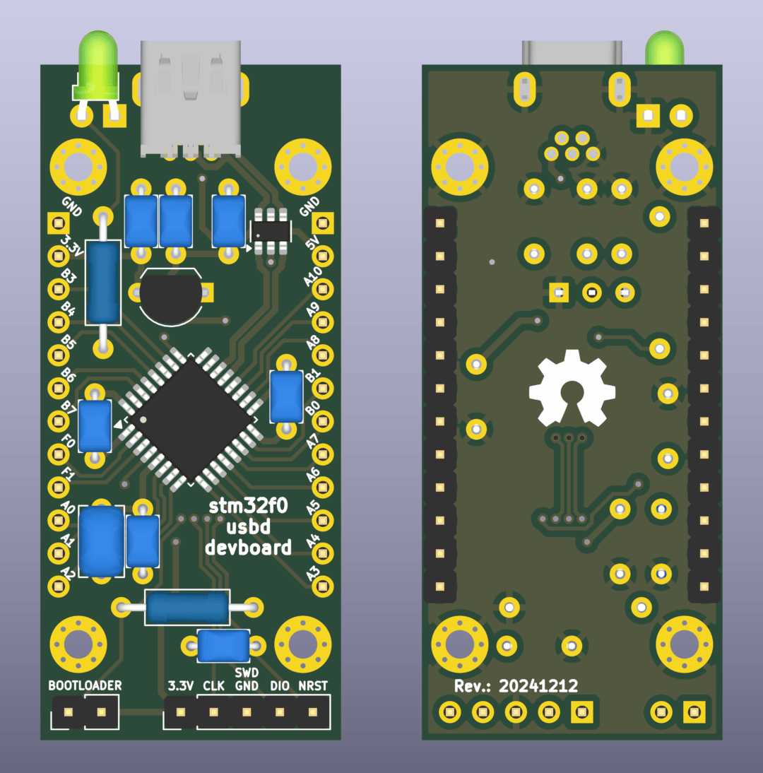
STM32F0 USB Development Board (revision 20241212)
Resources: