STM32G4
Table of contents
The STM32G4 variant is based on the STM32G431K6T6/K8T6/KBT6 (ARM Cortex-M4 with single-precision FPU, 170 MHz). It provides significantly more processing power than the F0 and C0 variants, with up to 128 KB of flash and hardware floating-point support.
Current revision (20250412)
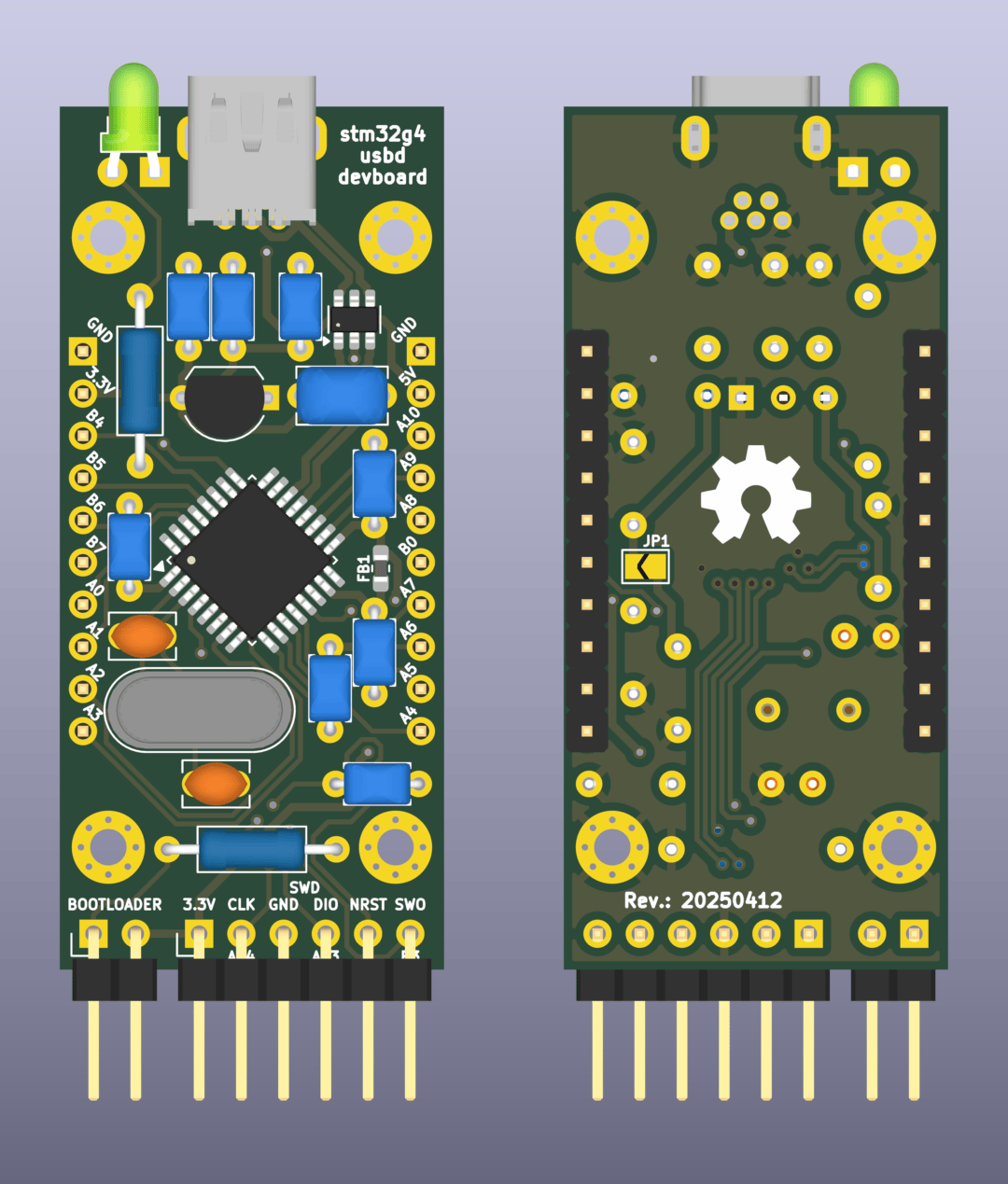
STM32G4 USB Development Board
Resources:
KiCad source files are available in the repository under pcb/stm32g4-usbd-devboard/. A KiCad symbol for this board (stm32g4-usbd-devboard) is provided in symbols/stm32-usbd-devboards.kicad_sym.
Supported microcontrollers
All three parts share the same LQFP-32 package and pinout, differing only in flash size. They use the CMSIS device identifier STM32G431xx.
| Part number | Flash | RAM |
|---|---|---|
| STM32G431K6T6 | 32 KB | 32 KB |
| STM32G431K8T6 | 64 KB | 32 KB |
| STM32G431KBT6 | 128 KB | 32 KB |
Warning
The CMSIS device identifier selects headers and startup code, but the linker script determines the memory layout. STM32G431xx covers all three parts above despite their different flash sizes. You must use a linker script that matches the actual chip populated on your board -- using a linker script for a larger flash variant will compile and link without errors but may produce firmware that writes beyond the physical flash.
Pinout
The board breaks out GPIO and power across two 1x10 pin headers (2.54 mm pitch), one on each side. PF0/PF1 are dedicated to the 24 MHz HSE crystal on this variant and are not available on the pin headers.
| J3 (Left) | Pin | J4 (Right) |
|---|---|---|
| GND | 1 | GND |
| 3V3 | 2 | +5V |
| B4 | 3 | A10 |
| B5 | 4 | A9 |
| B6 | 5 | A8 |
| B7 | 6 | B0 |
| A0 | 7 | A7 |
| A1 | 8 | A6 |
| A2 | 9 | A5 |
| A3 | 10 | A4 |
Clocking
The STM32G4 supports crystal-free USB operation via HSI48 with the Clock Recovery System (CRS), which uses USB SOF packets from the host to keep HSI48 within USB tolerance -- the same mechanism used on the F0 and C0 variants.
However, unlike on the F0 and C0, HSI48 cannot be used as the system clock or as the PLL source on the G4. When no HSE crystal is installed, the system clock must come from HSI -- the internal 16 MHz RC oscillator -- directly or via PLL. RC oscillators drift with temperature and supply voltage, so system clock accuracy in this configuration depends entirely on HSI's tolerance. CRS keeps USB working, but any other timing-sensitive function (UART baud rates, ADC sampling, timers) inherits that drift.
The optional 24 MHz HSE crystal (Y1) provides a stable, accurate clock reference for the system and is recommended. When installed, the PLL can derive both the system clock and a 48 MHz USB clock from the HSE input, and HSI48 is not needed.
Power filtering
Ferrite bead FB1 (600 ohm @ 100 MHz, 0603 SMD) is placed on the analog/USB power rail for noise filtering.
Solder bridge JP1 ("No FB1") can be closed to bypass FB1 if the ferrite bead is unavailable or unnecessary for the application. JP1 is open by default.
Note
This power filtering arrangement is unique to the G4 variant.
SWD, SWO, and DFU bootloader
SWD header (J2) -- 6-pin horizontal header with the following signals:
| Pin | Signal |
|---|---|
| 1 | 3V3 |
| 2 | SWCLK |
| 3 | GND |
| 4 | SWDIO |
| 5 | NRST |
| 6 | SWO |
SWO (Serial Wire Output) on PB3 provides trace output, enabling ITM-based printf-style debugging or tools like MCUViewer.
Bootloader header (J5) -- 2-pin horizontal header for BOOT0. Shorting the pins during power up activates the built-in USB DFU bootloader, allowing firmware flashing over USB without a hardware debugger.
For flashing instructions, refer to the generic Hardware Build Manual.
Board-specific build notes
- HSE crystal (Y1): 24 MHz, HC49 package. Optional, but recommended -- provides a more accurate clock reference for the system clock. Without it, USB still works via HSI48 with CRS, but HSI48 cannot be used as the system clock.
- Ferrite bead (FB1): 600 ohm @ 100 MHz, 0603 SMD. Recommended for mixed-signal applications. Can be bypassed by closing JP1.
- Solder bridge JP1: Open by default. Close only if FB1 is not installed.
- LED (D1): Green 3 mm PTH, horizontal mount.
For the complete build process, see the generic Hardware Build Manual.
Firmware development
For project setup, build system configuration, toolchain usage, and flashing instructions, refer to the cmake-cmsis-stm32 documentation. The CMSIS device identifier for this board is STM32G431xx.
For register-level details on peripherals, clocking, and CRS configuration, refer to the STM32G4 reference manual (RM0440).
Legacy revision: 20250402
This revision is nearly identical to the current one (20250412), with only minor fixes. The pinout, components, and functionality are the same.
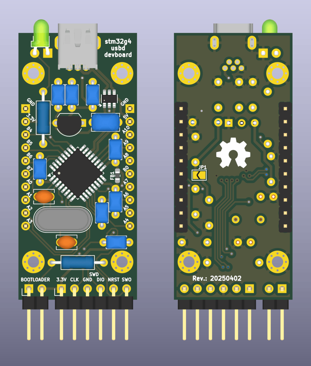
STM32G4 USB Development Board (revision 20250402)
Resources: